High-frequency PCB design is a specialized field that requires careful attention to signal integrity, impedance control, and electromagnetic interference (EMI) mitigation. Designing a PCB for high-frequency signals (typically above 100 MHz) or microwave frequencies (GHz range) demands a solid understanding of electrical engineering principles and the unique properties of materials and components at high frequencies.
Key Considerations in High-Frequency PCB Design:
1. Signal Integrity and Transmission Lines
Transmission Line Effects: At high frequencies, the PCB trace behaves like a transmission line, and signal degradation can occur if not properly designed. Transmission line impedance must be matched to the...
High-frequency PCB design is a specialized field that requires careful attention to signal integrity, impedance control, and electromagnetic interference (EMI) mitigation. Designing a PCB for high-frequency signals (typically above 100 MHz) or microwave frequencies (GHz range) demands a solid understanding of electrical engineering principles and the unique properties of materials and components at high frequencies.
Key Considerations in High-Frequency PCB Design:
1. Signal Integrity and Transmission Lines
Transmission Line Effects: At high frequencies, the PCB trace behaves like a transmission line, and signal degradation can occur if not properly designed. Transmission line impedance must be matched to the source and load impedance to avoid reflections.
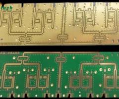
Impedance Control: The characteristic impedance (typically 50 ohms for RF signals) of traces should be precisely controlled. The design needs to ensure that trace width, spacing, and the dielectric material thickness are optimized for the desired impedance.Microstrip Lines: These are traces on the surface of the PCB, with a reference plane (ground) below them.Stripline: Traces are sandwiched between two ground planes, providing better shielding and lower susceptibility to external EMI.Coplanar Waveguides: Similar to microstrips, but with the ground plane adjacent to the signal trace.
2. Material Selection
High-frequency PCBs require materials with low loss and stable dielectric properties at high frequencies:
PTFE-based materials like Rogers laminates, Teflon, and ceramic materials are common choices because they offer low loss and stable electrical performance.
FR-4 can be used for lower-frequency applications, but higher-performance materials are preferred for GHz designs due to the higher loss tangent of FR-4 at high frequencies.
3. Component Placement
Minimize Trace Lengths: The shorter the trace, the lower the loss and the higher the signal integrity. High-frequency signals degrade over distance due to resistance, capacitance, and inductance.
Strategic Grounding: Grounding is crucial for high-frequency PCBs. Poor grounding can cause noise, EMI, and ground bounce. Ensure the PCB has a solid, continuous ground plane and use via stitching to connect the ground planes together.
Decoupling Capacitors: These are used to filter out noise from power supply lines. At high frequencies, the placement of decoupling capacitors should be as close as possible to the components to reduce inductance.
4. Cross-Talk and EMI Control
Reduce Cross-Talk: Cross-talk between adjacent signal traces can cause unwanted coupling of signals. To minimize this, maintain a sufficient distance between traces carrying high-speed signals or use ground planes to shield them.
EMI Shielding: High-frequency designs are more susceptible to EMI. Techniques like using shielding cans, keeping high-frequency traces short, and maintaining a continuous ground plane can help mitigate EMI. Additionally, proper via placement and PCB layer stacking are critical in controlling the return currents of high-frequency signals.
5. Via Design
Via Inductance: Vias introduce inductance, which can degrade signal integrity at high frequencies. Microvias (small vias) and buried vias are used to reduce the inductance of traditional vias.
Via Size: Keep via sizes small to reduce their impact on the signal path. A smaller via reduces its inductance, making it less of a bottleneck at high frequencies.
6. Thermal Management
High-frequency signals generate heat, so thermal management is crucial in high-frequency PCB designs. Ensure that heat can dissipate from components and traces by using thermal vias, heat sinks, and adequate spacing between high-power components.
In some cases, ceramic PCBs are used because of their excellent thermal conductivity.
7. Simulation and Testing
Simulations: Use simulation tools like HFSS, ADS (Advanced Design System), and Ansys to simulate the behavior of high-frequency circuits before fabrication. This helps to verify signal integrity, impedance matching, and EM radiation.
Prototyping and Testing: After fabrication, high-frequency PCBs should be tested using tools like vector network analyzers (VNA) and time-domain reflectometers (TDR) to measure the reflection and loss of signals at various frequencies.