High Density PCB board (HDI PCB) Manufacturer & Assembly – One-stop services
sales12@hitechpcb.com
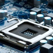
What’s HDI PCB?
High-density interconnect (HDI) PCBs are characterized by finer lines, closer spaces, and more dense wiring, which allow for a faster connection while reducing the size and bulk of a project. These boards also feature blind and buried vias, laser ablated microvias, sequential lamination, and via in-pads.
As a result, a HDI board can house the functionality of the previous boards used. HitechPCB is an HDI PCB manufacturer and provider in Shenzhen,Chinasupports HDI PCB prototype and mass production with less expensive price and quick-turn lead time. Customers from a variety of ind...
High Density PCB board (HDI PCB) Manufacturer & Assembly – One-stop services
sales12@hitechpcb.com
What’s HDI PCB?
High-density interconnect (HDI) PCBs are characterized by finer lines, closer spaces, and more dense wiring, which allow for a faster connection while reducing the size and bulk of a project. These boards also feature blind and buried vias, laser ablated microvias, sequential lamination, and via in-pads.
As a result, a HDI board can house the functionality of the previous boards used. HitechPCB is an HDI PCB manufacturer and provider in Shenzhen,Chinasupports HDI PCB prototype and mass production with less expensive price and quick-turn lead time. Customers from a variety of industries we serve have a common that have high expectations in quality, reliability and on-time delivery in HDI PCB production. Our quality is not afterthought, but built into each process from front-end to fabrication and shipping.
HDI PCB board
HDI PCB Manufacturing Process
The overall process for manufacturing HDI PCB is essentially the same as for fabricating other PCB board, with notable differences for PCB stack-up and hole drilling. Since HDI boards generally require smaller drill holes for vias, laser drilling is usually required. Although laser drills can produce smaller and more precise holes, they are limited by depth. Therefore, a limited number of layers can be drilled through at a time. For HDI boards, which are invariably multilayer and may contain buried and blind vias, multiple drilling processes may be required. This necessitates successive layer boding to achieve the desired stack-up or sequential lamination cycles. Not surprisingly, this can significantly increase PCB manufacturing time and cost.
HDI PCB fabrication is an advanced technology and therefore requires expertise along with specialized equipment like laser drills, laser direct imaging (LDI) capability, and special clean room environments. In order to efficiently manufacture high-quality and reliable HDI PCB products, you must understand the HDI board manufacturing process and coordinate with your HDI PCB supplier to implement good DFM (Design for Manufacturability) for HDI layout design.