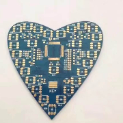
Designing high-frequency PCBs presents several unique challenges compared to traditional PCB design, primarily due to the way high-frequency signals behave. The primary challenges stem from signal integrity, impedance control, electromagnetic interference (EMI), and the need for precise materials and manufacturing processes. Below, I’ve outlined some common challenges in high-frequency PCB design along with practical solutions to address them.
1. Signal Integrity Challenges
Challenge: At high frequencies, signals become more sensitive to the PCB design. Any slight imperfections or deviations in the PCB layout — such as trace width, routing, or spacing — can result in signal distortion, reflections, or los...
Designing high-frequency PCBs presents several unique challenges compared to traditional PCB design, primarily due to the way high-frequency signals behave. The primary challenges stem from signal integrity, impedance control, electromagnetic interference (EMI), and the need for precise materials and manufacturing processes. Below, I’ve outlined some common challenges in high-frequency PCB design along with practical solutions to address them.
1. Signal Integrity Challenges
Challenge: At high frequencies, signals become more sensitive to the PCB design. Any slight imperfections or deviations in the PCB layout — such as trace width, routing, or spacing — can result in signal distortion, reflections, or loss. Signal degradation is more noticeable as the frequency increases, leading to errors and reduced performance.
2. Electromagnetic Interference (EMI) and Cross-Talk
Challenge: At high frequencies, signal lines can radiate electromagnetic waves, and these waves can interfere with adjacent traces or external systems. Cross-talk between signal traces can cause unintended coupling, leading to degraded signal quality.
3. Impedance Control
Challenge: Inconsistent or improper impedance matching is one of the leading causes of signal reflection, which can significantly degrade signal quality, especially in high-frequency applications like RF circuits.
4. Via Inductance and Parasitic Effects
Challenge: High-frequency signals are very sensitive to parasitic inductance and capacitance, especially in vias. Vias can introduce unwanted inductive reactance, which increases with frequency and negatively impacts signal integrity.
5. Thermal Management
Challenge: High-frequency designs often involve high-power components that generate significant heat. If not properly managed, excessive heat can degrade the performance of components and materials and may lead to circuit failure.
6. Fabrication Complexity and Cost
Challenge: High-frequency PCBs often require more specialized fabrication techniques compared to standard PCBs. These include using advanced materials like PTFE, ceramics, and hybrid laminates, which can drive up the cost and complexity of the manufacturing process.
7. PCB Materials Selection
Challenge: Choosing the wrong PCB material can lead to high losses, poor signal integrity, and other performance issues. Materials with higher loss tangents (e.g., FR-4) are not suitable for high-frequency applications as they increase signal attenuation.


